About
Quantum technology (QT) utilises the discrete states and dynamics of physical systems for practical applications.
Many of the devices that we use in on daily lives are actually based on controlled quantum phenomena, that are well known by the scientist for more than a century.
Examples of such technologies are transistors, light emitting diodes (LEDs), photodetectors, lasers, GPS/atomic clocks, MRI/MEG scanners for medical imaging and solar panels.
However, there are a number of peculiar quantum phenomena, such as entanglement and superposition, that only today are understood well enough to be translated into real life applications.
This change is not happening by chance but is based on decades of persistent work to understand the quantum realm, to develop fabrication processes and methods for nano-scale devices that can be used to run experiments on these phenomena in laboratory environment, and to develop theories and computational methods that help to interpret and understand what is really happening and what could be achieved next.
“Quantum Technology 2.0”, that aims at harnessing these phenomena, represents a completely new set of standards, where device performance is not limited by the classical laws of physics but instead is described by more versatile quantum dynamics.
QT 2.0 permits more powerful computing, provably secure communication technologies, unmatched simulation capabilities, higher sensitivity and precision sensing and new measurement types, from atomic up to macroscopic length scales. It provides unparalleled technological and societal impacts in sectors ranging from high performance computing to secure telecommunications and from chemistry/medicine to energy.
 1
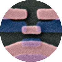
1Atomic scale quantum phenomena are studied in nanostructures fabricated at our laboratories.
 2
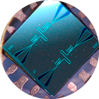
2These structures are compiled into circuits and devices that allow development of new components, sensors and detectors for quantum technology applications.
 3
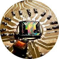
3The circuits are characterized and measured in setups that allow control of charge, flux, microwave radiation, phonons and photons at the ultimate accuracy.
 4
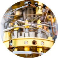
4Measurements are usually implemented in close-to-absolute-zero temperatures by utilizing refrigeration technologies originally developed at our laboratories.
 5
5Emergence of novel technologies builds on our broad experimental and theoretical expertise in low temperature physics, quantum phenomena and systems, as well as industrial-level production of superconducting sensors operating in deep-mK regime.
QTF builds on a long tradition in the chain of Centres of Excellence since the establishment of this programme in Finland in 1995.
The centre is formed around eleven strong research groups focusing on experiments on single quanta in solid state and device physics, theory of open quantum systems, and engineering capability to implement quantum technology.
QTF is a global leader in thermodynamics and control of heat in quantum circuits, thermal microwave detection on hybrid devices made out of 1D and 2D materials cooled down into deep-mK regime, as well as on industrial-level production of superconducting sensors. It brings together the national key players to lead Finland into the era of QT 2.0.
Scientific Advisory Board
QTF has a scientific advisory board (SAB) nominated by the Academy of Finland Research Council for Natural Sciences and Engineering. The SAB reviews the scientific progress of the CoE regularly and provides valuable support for its development.
QTF Scientific Advisory Board (from left to right):
Professor William Oliver, MIT, USA
Professor Dr. Christoph Bruder, University of Basel, Switzerland
Professor Jeanie Lau, The Ohio State University, USA
Observers participating in the activities of the SAB:
Dr. Sami Heinäsmäki, Grant Writer, Research and Innovation Services, Aalto
Prof. Heikki Tenhu, Vice Dean, University of Helsinki
Dr. (Tech.) Tauno Vähä-Heikkilä, Vice President, VTT
Prof. Ari Jokinen (University of Jyväskylä), Academy of Finland Research Council for Natural Sciences and Engineering
Dr. Timo Lehtinen, Academy of Finland Natural Sciences and Engineering Research Unit
(2018-2020 Prof. Kalle-Antti Suominen, Vice-Rector, Research, University of Turku)

National research infrastructure
QTF partners are among the leading developers of the national open access research infrastructure (RI) OtaNano, founded and developed jointly by AALTO and VTT.
OtaNano is included in the roadmap for national infrastructures in Finland 2021–2024, and it provides advanced nanofabrication, nanomicroscopy, and ultra-low temperature measurement facilities for quantum technologies on Otaniemi campus, Espoo.
OtaNano facilities have been developed over twenty years in European large-scale infrastructure collaboration, currently enforced as the European Microkevin Platform (EMP). The EMP underpins quantum technologies and nanoelectronics research in QTF with developments in the state-of-the art cryogenics and low noise measurement facilities.
OtaNano is an active high-tech environment combining industrial and academic research. Annually, nearly 500 users utilize the facilities, and, at present, over 30 companies collaborate in OtaNano exploiting the facilities of this RI.